| Specifications - Product No. G180000000QRSUPN43AB |
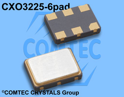
| Holder Type: |
CXO3225PK3.3; 3.3V(Voltage code is "3.3"); Tri-State on pad 1 |
| Frequency: |
180.000000 MHz |
| Frequency Stability at 25°C: |
± 25.0 ppm |
| Operating Temperature Range: |
± 25.0 ppm over -40°C to +85°C (incusive of 25°C tolerance,
±10% input voltage variation, load change, aging, shock and vibration ) |
| Storage Temperature: |
-55°C to +150°C |
| Power Supply Voltage (Vdd): |
+ 3.3V D.C. ± 5% |
| Maximum Supply Current (15pF load): |
30.0 mA typ. |
| Output Logic Levels: |
High "1" Voh Vdd-1.025V min., Vdd-0.95 V typical;
Vdd-0.88V max. Condition: RL= 50 Ohm to (Vdd-2.0V)
Low "0" VoL Vdd-1.810V min., Vdd-1.70 V typical;
Vdd-1.62V max. Condition: RL= 50 Ohm to (Vdd-2.0V) |
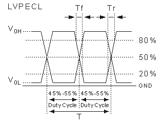
| Output Swing: |
595 mV min; 750 mV typical; 930 mV max. |
| Output Symmetry (Duty Cycle): |
50% ± 5%max. measured at 50% waveform |
| Load: |
RL=50 Ohm into (Vdd-2.0V) or
Thevenin equivalent (terminating resistors required on all outputs). |
| Rise/Fall Time: |
Tr = 0.3ns typical, 0.5ns max. @ 20% -> 80% of PECL wave form
Tf = 0.3ns typical, 0.5ns max. @ 80% ->20% of PECL wave form |
| Start Up Time: |
3 ms typical; 10 ms max. |
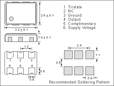
| OE Function Pin 1: |
Enable ll When 70% min. of VDD to Enable Output. Enable time : 10 ms max.
Disable ll When 30% max. of VDD to Disable Output.
Disable current : 10 µA max. , Disable time : 0.2 µs max. |
| Tri-state Function Pin 1 (or 2): |
If no connection or Vdd *70% min is applied: Output. Internal pull-up
Oscillation disable time is 2ms max.
If Vdd*30% max is applied: High impedance. 10µA typ., enable time 2ms max. |
| Phase Jitter (12 kHz to 20 MHz): |
0.2 ps typical, 0.5 ps (max.), for 156.250 MHz, 3.3V |
| Phase Noise (125 MHz): |
-50dBc/Hz @ 10Hz, -80dBc/Hz @ 100Hz, -115dBc/Hz @ 1kHz
-135dBc/Hz @ 10kHz, -142dBc/Hz @ 100kHz, -147dBc/Hz @ 1MHz,
-152dBc/Hz @ 10MHz |
| Aging: |
< ±3ppm max. for the first year |
| Reflow Condition: |
260°C max for 10 sec. |