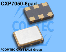
| Specifications - Product No. G025000000HVSUPN43AB |
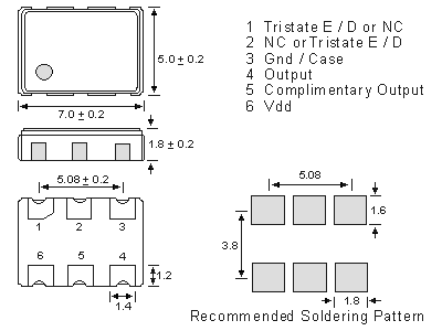
| Holder Type / Voltage (Vdd): |
CXO7050DQN3.3; + 3.3V D.C. ± 5%; Tri-State on pad 1 |
| Frequency: |
25.000000 MHz |
| Frequency Stability at 25°C: |
± 25.0 ppm |
| Operating-//Storage -Temperature Range: |
± 25.0 ppm , -40°C to +85°C // -55°C to +150°C |
| Maximum Supply Current: |
16mA typical |
| Output Logic: |
"High",1: 1.4V(typical); 1.6V (max.), RL = 100 Ohm
"Low ",0: 0.9V (min); 1.1V (typical), RL = 100 Ohm |
| Output Voltage Swing: |
250mV min., 350 typ., 450mV max., RL = 100 Ohm |
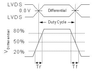
| Output Logic Levels: |
High "1" 90% of Vdd-min, Low "0" 10% Vdd-max.,
|
| Duty Cycle (50% Vdd): |
50% ± 5%max. |
| Load: |
100 Ohm between output and complimentary output |
| Rise (Tr)/Fall Time (Tf): |
0.2ns typical; 0.5ns max. (20%Vdd<->80% of the LVDS wave form) |
| Start Up Time: |
5 ms typical; 10ms max. |
| Tri-state Function Pin1(or2)No Connect.: |
Differential LVDS and complimentary LVDS outputs |
| Tri-state Disable: |
Both outputs are disabled (high impedance) when the Tri-state pad
taken below 0.45°C Vcc referenced to ground (threshold) Oscillator is
always On. Only Buffer stage is disabled. Disable current:50µA
max.(at0.0V), Disable Time 10ns (max.) |
| Tri-state Enable: |
At disabled mode, both outputs are enabled when the Tri-state pad
taken below 0.45°C Vcc referenced to ground (threshold)
Enable time: 10ms + one period of the output frequency (max.) |
| Phase Jitter: |
0.6 ps typ. (12 kHz to 20 MHz); < 100 fs (1.875 MHz to 20MHz) |
| Phase Noise (156.250 MHz): |
-67dBc/Hz @ 10Hz, -92dBc/Hz @ 100Hz, -112dBc/Hz @ 1kHz
-121dBc/Hz @ 10kHz, -124dBc/Hz @ 100kHz, -136dBc/Hz @ 1MHz,
-153dBc/Hz @ 5MHz |
| Aging: |
< ±2ppm max. for the first year; ±10ppm max. over 10 years |
| Reflow Condition: |
260°C max for 10 sec. |