| Specifications - Product No. G010000000CHSUPC00AA |
| Holder Type: |
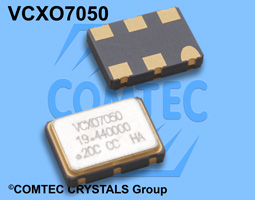
VCXO-Oscillator SMD VCXO7050T3.3-6pad 3.3V (Voltage code is "3.3" ) |
| Frequency: |
10.000000 MHz |
| Initial Freq. Accuracy (at 25 °C): |
To tune to the nominal frequency with Vc = 1.65V ±0.2V |
| Freq. Stability o.Operating Temp. Range: |
± 25.0 ppm |
| Operating Temperature Range: |
± 25.0 ppm over -20°C to +70°C (incusive of 25°C tolerance,
± 10% input voltage variation, load change, aging, shock and vibration ) |
| Deviation: |
Frequency Range ±100ppm |
| Power Supply Voltage (Vdd): |
+3.3V DC ± 10% |
| Maximum Supply Current: |
20.0 mA |
| Output Load CL: |
2 TTL gates max. / CMOS 15 pF |
| Output "1" Level (V0H): |
2.4V (min. ) TTL / 2.97V (min.) CMOS |
| Output "0" Level (V0L): |
0.4V (max.) TTL / 0.33V (max.) CMOS |
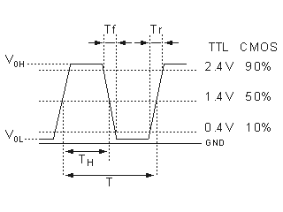
| Output Symmetry (Duty Cycle): |
40/60% |
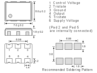
| Tri-State Function: |
Tri-State Enable High. No connection or Vdd- 0.5Vmin.is applied to a Tri-state
pin to enable output. Ground+0.5Vmax. to disable output (high impedance). |
| Modulation Bandwidth (at -3 dB): |
10KHz min, Vcontrol at 1.65V or at 2.5V |
| Voltage Control: |
1.65V DC Center / 0.3V to 3.0V Range |
| Linearity: |
6% typical; 10% max. |
| Rise/Fall Time TTL: |
6ns (max.) 4ns (typ.) Measured between 0.4V and 2.4V |
| Rise/Fall Time CMOS: |
6ns (max.) 4ns (typ.) Measured between 20% and 80% Vdd
of the wave form (CL = 15pF) |
| Integrated Phase Jitter: |
1 ps max. (12 kHz to 20 MHz) |
| Phase Noise (27MHz at 3.3V): |
-40dBc/Hz at 10Hz offset -147dBc/Hz at 10kHz offset
-104dBc/Hz at 100Hz offset -152dBc/Hz at 100kHz offset
-132dBc/Hz at 1kHz offset -150dBc/Hz at 1MHz offset |
| Start Up Time: |
10 ms (max.), 5ms (typ.) |
| Aging: |
±3 ppm per year (max.) |
| Input Impedance: |
1 M Ohm typical |
| Reflow Condition: |
10 sec. max. at 260°C |