| Specifications |
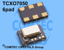
| Holder Type: |
TCXO7050PW3.3 3.3V(Voltage code is "3.3"); Tri-State on pad 2 |
| Frequency Range: |
10.0 MHz ~ 800 MHz |
| Standard Frequency (MHz, Partial List): |
10.000, 12.800, 16.000, 19.440, 20.000, 25.000, 27.000, 30.000, 32.000,
32.768, 38.880, 40.000, 50.000, 54.000, 64.000, 65.536, 77.760, 80.000,
100.00, 128.00, 155.52, 160.00, 200.00, 204.80, 311.04, 409.60, 622.08 |
| Freq. Stability vs Temperature: |
0° to 50°C (±1.0ppm) to -40 to +85°C ( ±3.0 to ± 5.0ppm) |
| Freq. Stability vs Aging: |
± 1.0 ppm, first year at 25°C |
| Freq. Stability vs Voltage Change: |
± 0.3 ppm, for a ± 5% input voltage change |
| Freq. Stability vs Load Change: |
± 0.3 ppm, for a ± 10% load condition change |
| Current Consumption (max.): |
10MHz? fout? 25MHz: 65mA (max); 25MHz ? fout ? 100MHz: 85mA (max);
100MHz ? fout? 800MHz: 115mA (max) |
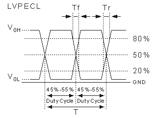
| Output Symmetry (Duty Cycle): |
50% ± 5% measured at Vdd-1.3V |
| Output Load: |
50 Ohm to Vdd-2.0V / CL = 15pF |
| Output Logic Levels: |
High"1"Voh=2.275Vmin Vdd-1.025min.,Condition: RL= 50 Ohm to (Vdd-2.0V)
Low"0" VoL=1.680Vmax Vdd-1.620max,Condition: RL= 50 Ohm to (Vdd-2.0V) |
| Rise/Fall Time: |
1.5ns max. @ 20% to 80% of PECL wave form |
| Start Up Time: |
5 ms (typ), 10.0ms (max.) (reach 90% amplitude and at+25°C ±2°C) |
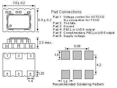
| Tri-state Funct. on Pin2, No Connection: |
Differential PECL and compliantary PECL outputs |
| Tri-state Function on Pin 2, Disable: |
Both outputs are disabled(high impedance) when pad 2 is taken below 0.45*Vcc
referenced to ground (threshold) Oscillator is always On. Only buffer stage is
disabled. Disable current: 50µA mac. (at 0.0V), Disable time: 10ns (max.) |
| Tri-state Function on Pin 2, Enable: |
At disabled mode , both outputs are enabled when Tri-state pad is taken above
0.45 Vcc referenced to ground (threshold);
Enable time: 10ns + one period of the output frequency (max.) |
| Phase Noise: |
Offset 10Hz 100Hz 1kHz 10kHz 100kHz
155.520 MHz :-65dBc/Hz -95dBc/Hz -120dBc/Hz -125dBc/Hz -121dBc/Hz
622.080 MHz :-55dBc/Hz -85dBc/Hz -109dBc/Hz -115dBc/Hz -110dBc/Hz
|
| Phase Jitter (RMS) (12 kHz to 20 MHz): |
2.6 ps typ., 4ps max., for 155.520MHz |
| Period Jitter (typical): |
Frequency Range: 38.880MHz 77.760MHz 155.520MHz 622.080MHz
(RMS): 2.2ps 3.5ps 4.3ps 5.0ps
(Peak to peak) : 17.0ps 25.0ps 27.0ps 32.0ps
|
| Temperature: |
Storage Temp. -55°C to +125°C / Reflow Condition 260°C max for 10 sec. |